Electronics Chips Find Hidden Flaws
📊Executive Summary
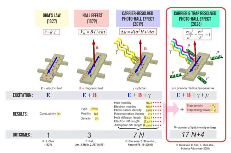
A new semiconductor analysis technique developed by KAIST and IBM significantly enhances the detection of hidden defects in electronic materials, achieving about 1,000 times greater sensitivity than traditional methods. This advancement allows for better identification of electronic traps that disrupt current flow, which can lead to performance issues in various semiconductor applications. The method improves efficiency in defect analysis by simultaneously measuring trap density and charge-transport parameters, potentially speeding up optimization and improving yields for devices like memory chips and solar cells. If widely adopted, this technology could reduce guesswork in defect mitigation and support the development of high-performance electronics....
More Insights Available
Unlock Full Analysis
Sign in to access the complete executive brief, risk analysis, and full article content.